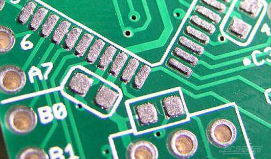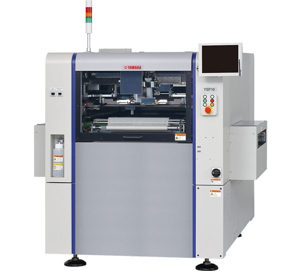
One of the most important parts of the surface mount assembly process is the application of solder paste to the printed circuit board (PCB). The aim of this process is to accurately deposit the correct amount onto each of the pads to be soldered. This is achieved by screen-printing the solder paste through a stencil or foil but also can be applied by jet printing. It is widely believed that this part of the process, if not controlled correctly, accounts for the majority of assembly defects.
To ensure the quality of the printing, it needs to monitor the printing press parameters: printing speed / squeegee pressure / printing gap / separation distance / clean frequency / paste thickness / the viscosity. All these parameters should be met the specification. The thinkness and viscosity of the paste should be also met the specification.
The specifications of the thickness of the stencil and tin coating:
0.12mm 0.11 ~ 0.17mm 0.18mm 0.15 ~ 0.23mm
0.15mm 0.13 ~ 0.21mm 0.20mm 0.17 ~ 0.25mm

Our Contacts
- Sector 63,Noida, Uttar Pradesh
- +91 70603 08061


