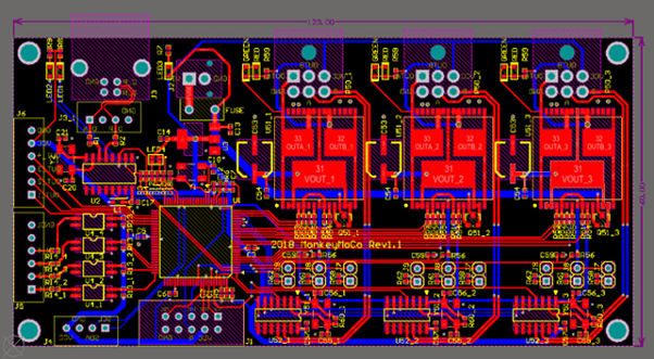
Once the blueprint has been completed, the PCB design comes next. The design is the layout, or physical representation of the PCB schematic and includes the copper track and hole layout. The PCB design does show the locations of the components as well as their connections with copper.
PCB design is the phase that’s concerned with performance. Engineers build the real components on top of the PCB design, allowing them to test whether the device works or not. We mentioned before that anyone should be able to understand a PCB schematic, but the functionality is not readily understood by looking at the prototype.
Printed circuit board (PCB) design brings your electronic circuits to life in the physical form. Using EDA tools, the PCB design process combines component placement and routing to define electrical connectivity on a manufactured circuit board.
The generic standard of printed circuit board is IPC-2221A and for PCB manufacturing its is IPC-6012B regardless of whether the PCB board is single sided; double sided or multi layered and while designing you shouldn't forget this.
PCB Technocrats, uses the best and latest EDA tools to provide best in class engineering for our valuable customers.
Why PCB Technocrats :
- A pool of designers highly experienced in the usage of PCB Layout Design software.
- We are customer centric, and we work around your schedule to meet your requirements.


